- 您现在的位置:买卖IC网 > Sheet目录2008 > MAX1195ECM+TD (Maxim Integrated Products)IC ADC 8BIT 40MSPS DL 48-TQFP
MAX1195
Dual, 8-Bit, 40Msps, 3V, Low-Power ADC with
Internal Reference and Parallel Outputs
_______________________________________________________________________________________
5
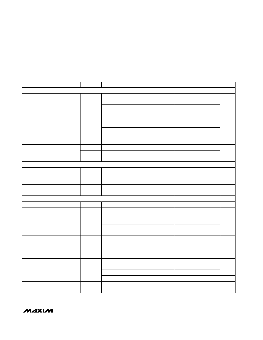
PARAMETER
SYMBOL
CONDITIONS
MIN
TYP
MAX
UNITS
DIGITAL INPUTS (CLK, PD,
OE, SLEEP, T/B)
CLK
0.8
×
VDD
Input High Threshold
VIH
PD,
OE, SLEEP, T/B
0.8
×
OVDD
V
CLK
0.2
×
VDD
Input Low Threshold
VIL
PD,
OE, SLEEP, T/B
0.2
×
OVDD
V
Input Hysteresis
VHYST
0.15
V
IIH
VIH = VDD = OVDD
±20
Input Leakage
IIL
VIL = 0
±20
A
Input Capacitance
CIN
5pF
DIGITAL OUTPUTS ( D7A–D0A, D7B–D0B)
Output Voltage Low
VOL
ISINK = -200A
0.2
V
Output Voltage High
VOH
ISOURCE = 200A
OVDD
- 0.2
V
Three-State Leakage Current
ILEAK
OE = OVDD
±10
A
Three-State Output Capacitance
COUT
OE = OVDD
5pF
POWER REQUIREMENTS
Analog Supply Voltage Range
VDD
2.7
3
3.6
V
Output Supply Voltage Range
OVDD
CL = 15pF
1.7
3
3.6
V
Operating, fINA & B = 20MHz at
-1dB FS applied to both channels
29
36
Sleep mode
3
mA
Analog Supply Current
IVDD
Shutdown, clock idle, PD =
OE = OVDD
0.1
20
A
Operating, fINA & B = 20MHz at
-1dB FS applied to both channels (Note 6)
8mA
Sleep mode
3
Output Supply Current
IOVDD
Shutdown, clock idle, PD =
OE = OVDD
310
A
Operating, fINA & B = 20MHz at
-1dB FS applied to both channels
87
108
Sleep mode
9
mW
Analog Power Dissipation
PDISS
Shutdown, clock idle, PD =
OE = OVDD
0.3
60
W
Offset, VDD
±5%
±3
Power-Supply
Rejection
PSRR
Gain, VDD
±5%
±3
mV/V
ELECTRICAL CHARACTERISTICS (continued)
(VDD = OVDD = 3V, 0.1F and 2.2F capacitors from REFP, REFN, and COM to GND; REFOUT connected to REFIN through a 10k
resistor, VIN = 2VP-P (differential with respect to COM), CL = 10pF at digital outputs, fCLK = 40MHz, TA = TMIN to TMAX, unless
otherwise noted.
≥+25°C guaranteed by production test, <+25°C guaranteed by design and characerization. Typical values are at
TA = +25°C.)
发布紧急采购,3分钟左右您将得到回复。
相关PDF资料
MAX1197ECM+TD
IC ADC 8BIT 60MSPS DL 48-TQFP
MAX1202AEPP+
IC ADC 12BIT 8CH 20-DIP
MAX121EAP+
IC ADC 14BIT 308KSPS 20SSOP
MAX1238MEEE+T
IC ADC 12BIT SERIAL 16-QSOP
MAX1240AEPA+
IC ADC 12BIT SERIAL 8-DIP
MAX1245BCPP
IC ADC SRL 12BIT 2.375V 20-DIP
MAX1249AEPE+
IC ADC 10BIT SERIAL 16-DIP
MAX1279AETC+
IC ADC 12BIT 1.5MSPS 12-TQFN
相关代理商/技术参数
MAX1195ECM-D
功能描述:模数转换器 - ADC RoHS:否 制造商:Texas Instruments 通道数量:2 结构:Sigma-Delta 转换速率:125 SPs to 8 KSPs 分辨率:24 bit 输入类型:Differential 信噪比:107 dB 接口类型:SPI 工作电源电压:1.7 V to 3.6 V, 2.7 V to 5.25 V 最大工作温度:+ 85 C 安装风格:SMD/SMT 封装 / 箱体:VQFN-32
MAX1195ECM-TD
功能描述:模数转换器 - ADC RoHS:否 制造商:Texas Instruments 通道数量:2 结构:Sigma-Delta 转换速率:125 SPs to 8 KSPs 分辨率:24 bit 输入类型:Differential 信噪比:107 dB 接口类型:SPI 工作电源电压:1.7 V to 3.6 V, 2.7 V to 5.25 V 最大工作温度:+ 85 C 安装风格:SMD/SMT 封装 / 箱体:VQFN-32
MAX1196ECM
制造商:Rochester Electronics LLC 功能描述: 制造商:Maxim Integrated Products 功能描述:
MAX1196ECM+D
功能描述:模数转换器 - ADC 8-Bit 2Ch 40Msps 3V High Speed ADC RoHS:否 制造商:Texas Instruments 通道数量:2 结构:Sigma-Delta 转换速率:125 SPs to 8 KSPs 分辨率:24 bit 输入类型:Differential 信噪比:107 dB 接口类型:SPI 工作电源电压:1.7 V to 3.6 V, 2.7 V to 5.25 V 最大工作温度:+ 85 C 安装风格:SMD/SMT 封装 / 箱体:VQFN-32
MAX1196ECM+TD
功能描述:模数转换器 - ADC 8-Bit 2Ch 40Msps 3V High Speed ADC RoHS:否 制造商:Texas Instruments 通道数量:2 结构:Sigma-Delta 转换速率:125 SPs to 8 KSPs 分辨率:24 bit 输入类型:Differential 信噪比:107 dB 接口类型:SPI 工作电源电压:1.7 V to 3.6 V, 2.7 V to 5.25 V 最大工作温度:+ 85 C 安装风格:SMD/SMT 封装 / 箱体:VQFN-32
MAX1196ECM-D
功能描述:模数转换器 - ADC RoHS:否 制造商:Texas Instruments 通道数量:2 结构:Sigma-Delta 转换速率:125 SPs to 8 KSPs 分辨率:24 bit 输入类型:Differential 信噪比:107 dB 接口类型:SPI 工作电源电压:1.7 V to 3.6 V, 2.7 V to 5.25 V 最大工作温度:+ 85 C 安装风格:SMD/SMT 封装 / 箱体:VQFN-32
MAX1196ECM-TD
功能描述:模数转换器 - ADC RoHS:否 制造商:Texas Instruments 通道数量:2 结构:Sigma-Delta 转换速率:125 SPs to 8 KSPs 分辨率:24 bit 输入类型:Differential 信噪比:107 dB 接口类型:SPI 工作电源电压:1.7 V to 3.6 V, 2.7 V to 5.25 V 最大工作温度:+ 85 C 安装风格:SMD/SMT 封装 / 箱体:VQFN-32
MAX1197ECM
制造商:Rochester Electronics LLC 功能描述: 制造商:Maxim Integrated Products 功能描述: